- Share
- Share on Facebook
- Share on LinkedIn
She is in charge of the whole manufacturing chain of these micro-devices, after definition with the applicant. The main steps in the manufacturing of an impression are :
- shaping of the mask representing the circuit
- deposition of the photosensitive resin on a 3" silicon plate
- UV exposure and revelation of the circuit imprint
This step can be done in two ways: exposure through a mask, or direct laser writing, using a device purchased in 2019 (Dilase by Kloé) and if the applicant wants a finished product...
- molding of PDMS on this impression
- gluing on glass slide
- installation of the fluidic connection
|
 |
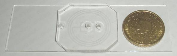 |
Below is an example of a SU8 mold before molding with PDMS resin (SU8 thickness of 140microns)
Contact
Scientific Manager
Gwennou COUPIER
Office 309
04 76 74 83 99
gwennou.coupier univ-grenoble-alpes.fr (gwennou[dot]coupier[at]univ-grenoble-alpes[dot]fr)
Deputy Scientific Manager
Philippe MARMOTTANT
Office 330
04 76 74 84 83
philippe.marmottantuniv-grenoble-alpes.fr (philippe[dot]marmottant[at]univ-grenoble-alpes[dot]fr)
Technical Team
Direct photolithography development
Mathilde VAN MELLE-GATEAU
Office 303
04 76 74 83 93
mathilde.gateauuniv-grenoble-alpes.fr (mathilde[dot]gateau[at]univ-grenoble-alpes[dot]fr)
Technical manager
Danièle CENTANNI
Office 201
04 76 74 82 84
daniele.centanniuniv-grenoble-alpes.fr (daniele[dot]centanni[at]univ-grenoble-alpes[dot]fr)
- Share
- Share on Facebook
- Share on LinkedIn